Key ideas
- •Today’s fastest chips are limited more by heat than by computing power.
- •Growing diamond in the right places could help electronics stay cooler and last longer.
- •If this scales, diamond might become a practical cooling layer inside future AI hardware.
One of the biggest challenges in advanced electronics today is keeping devices cool. Chips can get so hot that heat removal now limits performance more than the number or speed of transistors.
Researchers at Rice University have demonstrated a new way to grow diamond structures directly on semiconductor surfaces at the wafer scale, using a selective, bottom-up approach rather than adding pre-made diamond layers.
This method can lower temperatures by up to 23 degrees Celsius, and could be a major step forward in how chips are cooled.
Heat: the main barrier in modern electronics
Today’s high-performance electronics often run close to their thermal limits. For example, gallium nitride (GaN) transistors used in radar and 5G base stations handle very high power levels.
AI chips in data centers consume so much power that they can overheat quickly if heat isn’t well managed. Stacking chips on top of each other only makes the problem harder to solve.
Cooling needs to be built into the design. If heat builds up, chips become less reliable, run slower, or require larger, more expensive cooling systems.
Chips work better and last much longer when they stay cool. Lowering the temperature by just 10 degrees can add years to a chip’s lifespan.
The 23-degree temperature drop achieved by Rice could let chips run faster or need less cooling. Diamond might become an important part of future electronics.
Diamond carries heat about five times better than copper and more than ten times better than silicon. Using diamonds in chips could help them stay cooler and last longer.
The main challenge with using diamond isn’t its ability to conduct heat, but the technical difficulties of combining it with semiconductor systems.
Some key obstacles are ensuring the diamond sticks well, reducing heat resistance at material interfaces, and avoiding stress from differing rates of expansion. Growing even, defect-free diamond layers on large wafers is also a big engineering challenge.
Traditionally, engineers grew a full layer of diamond and then shaped it to fit onto chips.
Because diamond is so tough, this process is slow, requires extensive equipment, and can damage both the diamond and the chip. Making diamond layers big enough for today’s electronics is especially hard.
The Rice team developed a bottom-up approach to add diamonds to semiconductors. They start by using lithography to make tiny spots on the surface, marking exactly where diamond crystals will start to grow.
This method means there’s no need to shape the diamond after it forms. Instead, it lets engineers control exactly where the diamond goes, making it easier to fit with current chip-making processes.
Bottom-up patterned growth
This approach employs microwave plasma chemical vapor deposition (MPCVD). In this process, carbon-rich gases are transformed into plasma, enabling carbon atoms to deposit exclusively on pre-seeded substrate regions. Nucleation sites function as initiation points for diamond crystal growth.
The key improvement is in the seeding step. Using photolithography, researchers create precise patterns on the surface, marking where diamond seeds should be placed.
For bigger wafers, Rice researchers use a laser to pattern a thin film, taking it off only where they want diamond. They then add nanodiamond seeds to these open areas, creating a template for diamond to grow.
Now, engineers can place diamonds only where heat is highest, such as under powerful transistors or hotspots, instead of covering the entire wafer.
This method aligns with the industry’s move toward combining multiple chips and materials closely together in a single module.
As power, logic, and memory parts are packed closer together, managing heat well becomes even more important. For diamond to work at this scale, it needs to fit with current manufacturing methods, something Rice’s success with 2-inch wafers is making more possible.
Notably, DARPA is supporting this work, showing the government’s interest in more energy-efficient computing. This support suggests diamond could play a bigger role in future electronics, not just in research labs. no longer just a luxury material; it acts as a structural thermal layer within the device.
High-frequency, high-power transistors in radar, 5G, and communications often overheat. Adding a patterned diamond under these parts could improve cooling without needing a complete redesign.
High-performance GPUs and AI chips generate significant heat and often struggle with cooling. Spreading heat better on the chip can save energy and make data centers more reliable.
Scaling challenges
Challenges in scaling and in the interfaces between diamond and semiconductor materials must be addressed to efficiently transfer heat, requiring careful engineering to minimize thermal boundary resistance.
Also, diamond and other materials expand at different rates when heated, which can cause strain or defects. Getting diamonds to grow evenly across large wafers is still a tough technical challenge.
Moving from lab tests to making diamond work on full wafers is a big step, making it a real option for the industry. The next steps are to improve how diamond interfaces with other materials and to refine growth methods to maintain its excellent thermal properties.
Managing heat is now seen as a strategic issue, not just a technical one. Both defense and commercial devices, such as radar and energy systems, require more power in smaller spaces. Better heat removal means hardware lasts longer and works more reliably.
As computers need to do more, being energy efficient is becoming a major advantage.
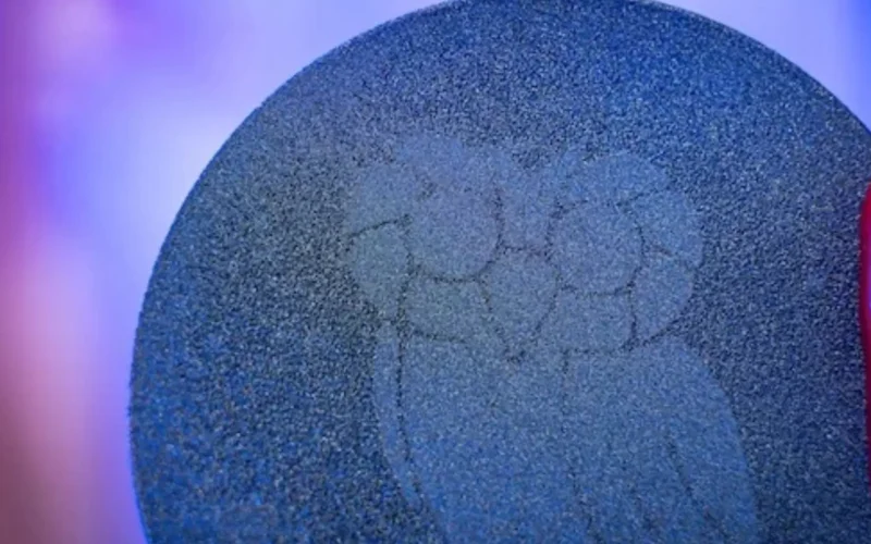
In early Rice experiments, the patterned diamond shapes were as artistic as they were scientific, showing that creativity and curiosity drive innovation. The real achievement is not just making patterns, but controlling exactly where and how diamonds grow on chips.
By changing how many diamond seeds they use, researchers can control the size and structure of the crystals, directing heat flow where it’s needed. This level of control adds a new layer to chip design, making the thermal parts as carefully planned as the electrical circuits.
This change is like how power networks in chips have evolved from simple wiring to complex, co-designed systems. Rice’s research doesn’t mean diamond will replace silicon, but it does show diamond could become a key tool for managing heat in advanced electronics.
As transistor miniaturization reaches limits, overcoming energy and thermal barriers is crucial. If scaling and technical challenges are addressed, diamond could become a key part of next-gen semiconductors.
The big question now is whether materials science can keep pace with the rapidly growing needs of modern computing. Diamond, once valued for its beauty and strength, may soon be prized for helping tomorrow’s electronics stay cool, efficient, and reliable.