Key ideas
- •Sony and TSMC are building image sensors that can process AI workloads directly on the chip instead of sending raw data to a central processor.
- •The partnership aims to create the vision layer for robots, autonomous vehicles, and other physical AI systems.
- •By combining Sony's sensor expertise with TSMC's advanced manufacturing, the companies are pushing machine vision closer to real-time decision making.
The smartphone you are holding in your hands, or that you are probably reading this article on, even if Sony hasn’t developed it, is equipped with a component from the company. That part is the image sensor in your phone’s camera. The same sensors are used across many applications, including traffic monitoring in self-driving cars and supporting surveillance drones and robots.
Sony Semiconductor Solutions controls about half of the global Complementary Metal-Oxide-Semiconductor (CMOS) image sensor market. CMOS sensors convert light into digital information for nearly every camera and vision system worldwide. Recently, Sony announced a joint venture with Taiwan Semiconductor Manufacturing Company (TSMC) to build the next generation of those sensors.
The partnership has brought together the world’s best sensor maker, Sony, with the world’s best chipmaker, TSMC, to give robots and self-driving cars eyes.
The problem with how machines see today
A CMOS image sensor consists of many tiny light-sensitive cells called photodiodes. Each cell measures the amount of light that hits it and turns that measurement into an electrical signal. When you stack millions of these cells together and read their signals quickly, you can create an image. For a smartphone camera, that is sufficient. The phone’s processor handles the rest, running computational photography algorithms, applying HDR processing, and identifying faces, making the sensor’s job limited to capturing light.
However, for a robot exploring a new area or a self-driving car speeding through the rain, the sensors need to do much more. Modern image sensors are complex semiconductor systems that include light sensors, advanced processing logic, memory, artificial intelligence capabilities, and specialized components for data readout. The main issue is the large amount of data these applications create. A single high-resolution automotive camera can generate several gigabytes of image data every second. If a robot has four cameras, it produces four times as many images. Sending all this data to a central processor for analysis causes delays.
This delay, even if it’s only a fraction of a second, can be significant. At highway speeds, this delay can mean several meters of road ahead. In a factory, it can result in a faulty part being overlooked. In defense situations, it can lead to targeting decisions made with outdated information. The industry is moving towards processing data directly on the sensor, which means turning raw data into useful information before it leaves the chip. To do this, logic circuits need to be placed directly behind the photodiode layer, enabling AI to operate at the moment of capture rather than later.
However, to create these circuits with the density and efficiency needed for physical AI applications, advanced semiconductor manufacturing is necessary. Sony cannot provide this capability on its own, and that is where the company needs TSMC.
Sony-TSMC image sensor partnership
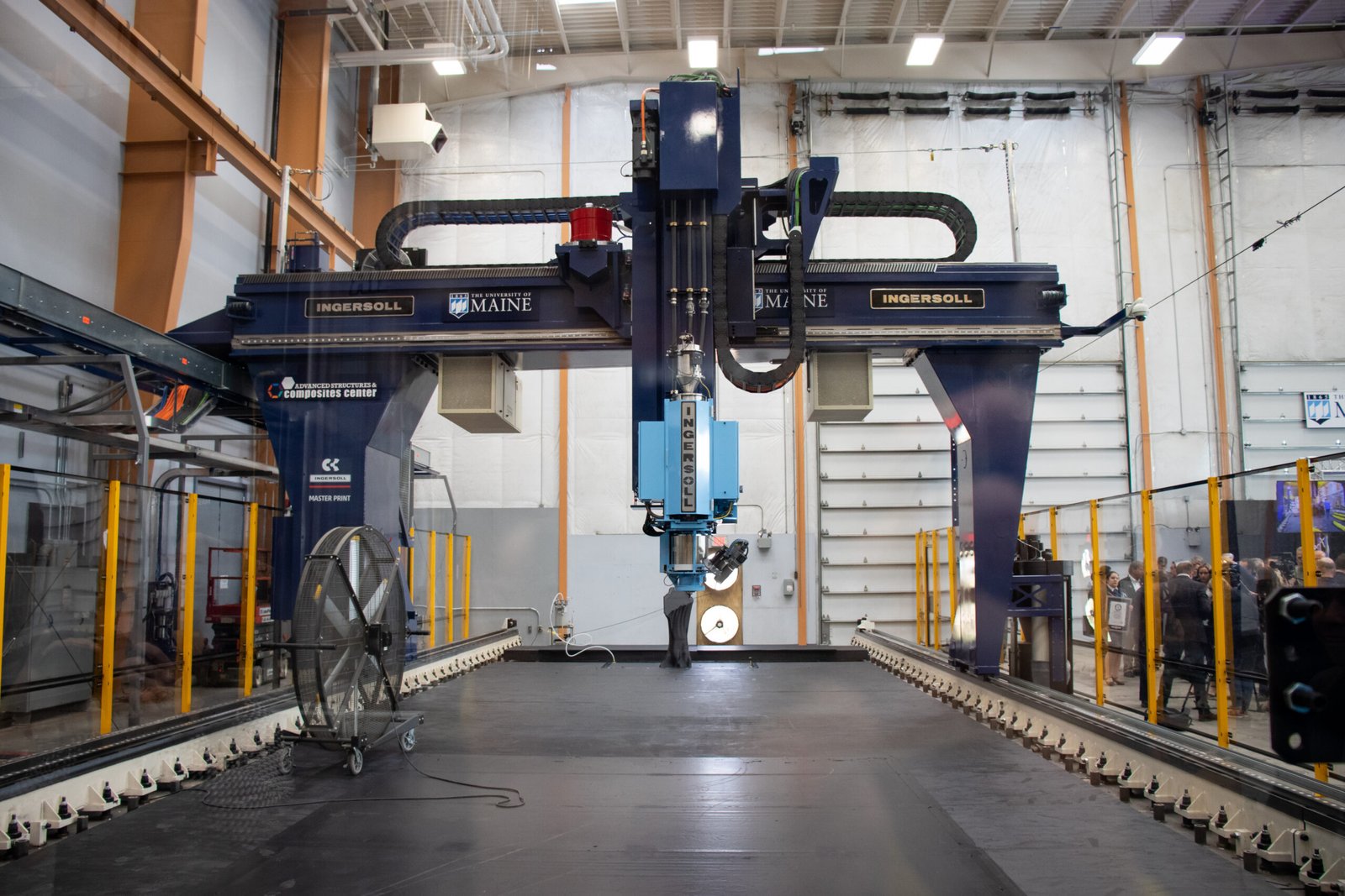
Sony Semiconductor Solutions and TSMC signed a memorandum of understanding on May 8, 2026, to establish a joint venture to develop and manufacture next-generation image sensors. Sony will be the majority and controlling shareholder. The JV will set up development and production lines at Sony’s newly constructed fab in Koshi City, Kumamoto Prefecture, with Sony also planning phased capital investment in its existing plant in Nagasaki, both of which will receive support from the Japanese government.
TSMC usually does not work with customers on joint product development and manufacturing. Instead, the company follows a foundry model. In this model, a customer provides a chip design, and TSMC manufactures it while keeping a separation between the two. A joint venture in which TSMC and the customer develop the product together is a different situation. This type of arrangement demonstrates that the technology combines Sony’s sensor design expertise with TSMC’s manufacturing capabilities in a way neither company can achieve on its own.
Sony excels in sensor design, while TSMC excels in advanced manufacturing processes. Together, they plan to focus on new opportunities in physical AI applications, specifically in automotive and robotics. “Building on the trust cultivated through our long-standing collaboration with TSMC, I am delighted that we have reached an agreement to advance our partnership to a new stage,” said Shinji Sashi`da, President and CEO of Sony Semiconductor Solutions.
“This JV is a significant initiative that brings together the strengths of both companies and aims to drive further advancement in technology and business within the next-generation image sensor field.”
“Sony has been our long-time partner in the CMOS image sensor business,” said TSMC Senior Vice President and Deputy Co-COO Dr. Kevin Zhang. “We are excited to elevate our collaboration to the next level, which represents a key step forward in driving future sensing technology in the AI era.”
How TSMC would create a difference
Sony’s latest smart sensor series, the IMX500, uses a two-layer design. The top layer captures light with photodiodes, while the layer below it processes the image using AI before sending out results, not raw data. The design reduces data output from a security camera by over 99%, while still allowing important information to be sent, such as detecting when a person crosses a line, rather than continuously sending every video detail.
Next-generation sensors improve on current technology by using stacked designs that require faster circuits and advanced processing layers, and TSMC’s manufacturing process supports these requirements. Creating a three-layer stack of photodiode, logic, and memory at the density needed for automotive and robotics requires manufacturing capabilities beyond what Sony can provide.
TSMC is upgrading its second Kumamoto facility to 3nm, the same technology used in smartphone chips and AI processors. It makes TSMC the best choice for manufacturing sensors that perform AI tasks in real time while handling the heat, vibration, and safety requirements of automotive environments.
The combination addresses a key issue that limits the practical use of physical AI. Robots and self-driving cars fail because the sensor data they rely on is too slow or requires too much processing in real-world situations. A sensor that uses its own AI to process data on board, running on advanced 3nm technology, helps to close this gap.
The Kumamoto answer
The companies’ choice of Kumamoto is also not incidental. Sony Semiconductor Solutions has invested in Japan Advanced Semiconductor Manufacturing, a TSMC subsidiary in Kumamoto Prefecture. The investment helps Sony strengthen its partnership with TSMC and ensures a steady supply of logic wafers for its stacked CMOS image sensors.
Sony is forming a joint venture with TSMC by opening a new factory in Koshi City, Japan. This factory is in the same area as TSMC’s Japanese facility, which puts them close to each other. Being nearby helps the top image sensor designer and the leading chip manufacturer work more closely together. It is easier and cheaper to move wafers between these nearby factories than to transport them across the Taiwan Strait, thereby reducing logistics costs and supply chain risks.
TSMC’s Kumamoto investment reinforces Japan’s role as a stable, advanced manufacturing base, and insulates the global supply chain from geopolitical disruptions. For a product as strategically important as the image sensor, which sits at the perception layer of autonomous vehicles, defense systems, industrial robots, and medical devices, supply chain geography matters.
Even the Japanese government is supporting the companies. The support for both the JV investment and the Nagasaki capital expansion places image sensor manufacturing in the same category of strategic industrial infrastructure that Japan has recently applied to logic chips through Rapidus and to memory through the revival of domestic NAND production.
The market
The image sensor market is expected to grow from $23.7 billion in 2026 to $37 billion by 2032. This is an annual growth rate of 7.7%. The demand for image sensors is increasing in consumer electronics, automotive, and industrial applications. In March 2026, McKinsey predicted that the overall sensor market could reach $45 billion by 2035. The LiDAR segment, in particular, will grow quickly as more advanced driver assistance systems and autonomous driving technologies are adopted.
These numbers show a big change in how we use image sensors. Sony describes its automotive camera business as providing the “eyes of vehicles.” These sensors help cars monitor their surroundings and detect obstacles. They are used in advanced driver assistance systems and automated driving systems.
Robots have the same requirement. A humanoid robot navigating a factory floor or a construction site needs depth perception, object recognition, and real-time response to a dynamic environment. A quadruped robot conducting military reconnaissance needs to operate in low light, adverse weather, and contested electromagnetic environments where radar-based sensing may be jammed. The image sensor and the AI processing architecture built into it determine what any of these systems can actually do in the world.
Sony controls roughly half of the global CMOS image sensor market, supplying sensors used in smartphone cameras and autonomous vehicles. Its sensors have long been used in Apple iPhones. That market position gives the Sony-TSMC JV a structural advantage that the sensors it develops will enter a supply chain that already routes through Sony’s existing customer relationships across automotive, consumer, industrial, and defense markets.
Physical AI is the phrase Jensen Huang used repeatedly during his two-week Asia tour last month to describe the next wave of AI deployment, systems that operate in the physical world, in factories, on roads, in warehouses, and on military platforms. During that tour, Huang signed partnerships with Hyundai for autonomous vehicles, with LG and Doosan for industrial robots, and with SK Hynix for the memory that powers those systems.
Each of those partnerships depends on a sensor layer that can observe the environment into which those AI systems are deployed. The Sony-TSMC joint venture is building that sensor layer for the physical AI applications that Huang signaled in Seoul.