Key ideas
- •Chinese researchers claim curcumin from turmeric improves precision in ceramic 3D printing by reducing UV-induced defects.
- •Adding curcumin helps absorb harmful UV light and prevents unwanted chemical reactions.
- •The advancement enables the production of complex, small-scale ceramic components crucial for semiconductors and electronics.
Many modern technologies, such as semiconductor manufacturing equipment, 5G networks, missile covers, and hypersonic vehicles, rely on advanced ceramics. These materials are strong, heat-resistant, electrically controllable, and stable in harsh environments that can damage metals and plastics. However, making them with precision is very challenging.
Researchers at Hunan University in China have claimed that they made progress in a manufacturing process by addressing a major challenge. They found a solution using a compound found in turmeric.
Professor Xiaoxiao Han and her co-workers recently reported in the International Journal of Extreme Manufacturing that curcumin, the pigment that gives turmeric its yellow color, resolves a fundamental light-scattering problem in ceramic 3D printing that has long constrained the precision of industrial ceramic components across multiple sectors. The finding does not focus on the ingredient itself. Instead, it highlights what the ingredient allows in the production process.
The problem that has been limiting ceramic manufacturing
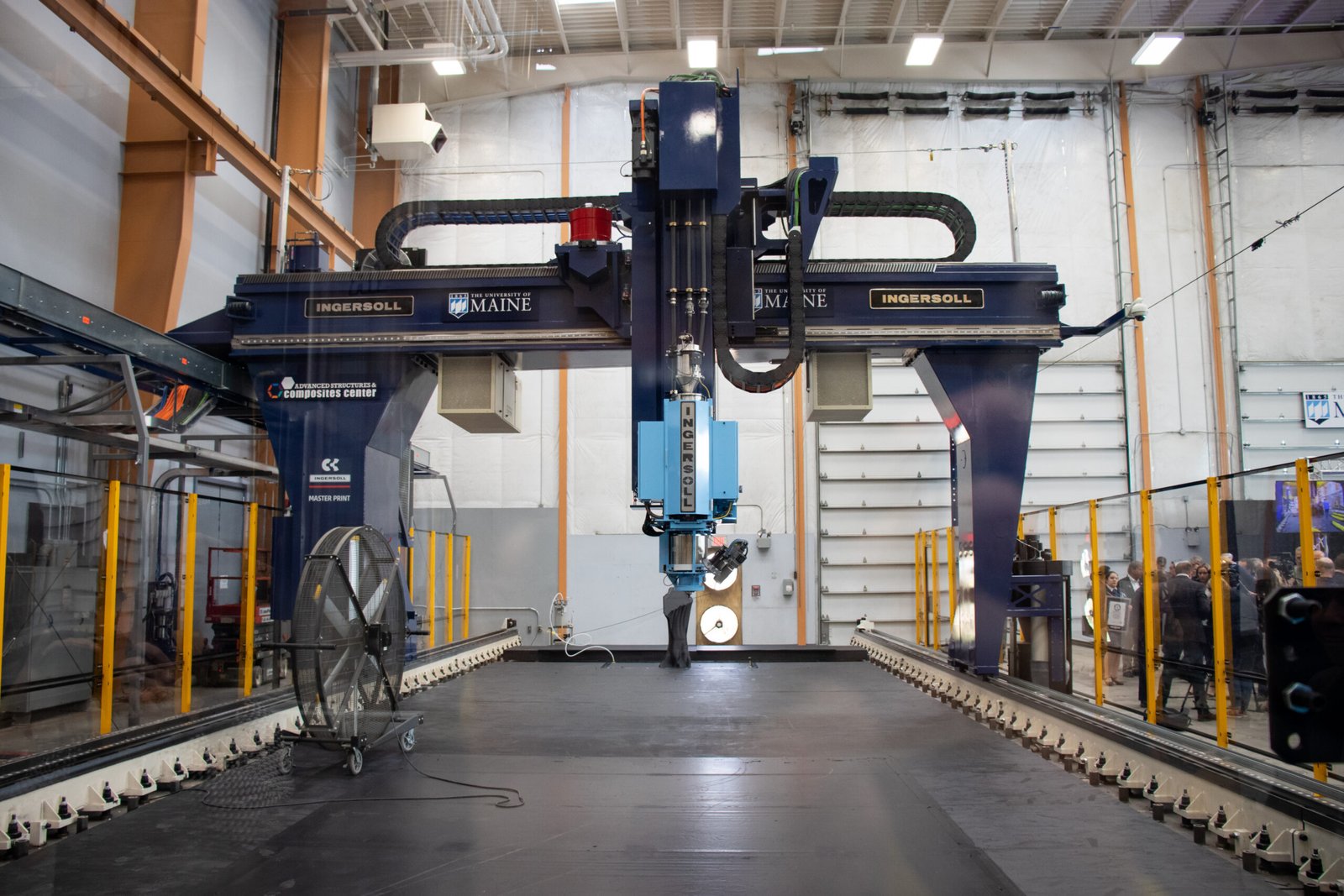
The main printing method in this research is digital light processing (DLP). It projects patterns of ultraviolet light into a liquid resin, which hardens layer by layer into a solid shape. DLP is fast and flexible, making it useful for creating complex shapes with high precision. It is commonly used in electronics manufacturing, aerospace, and medical devices.
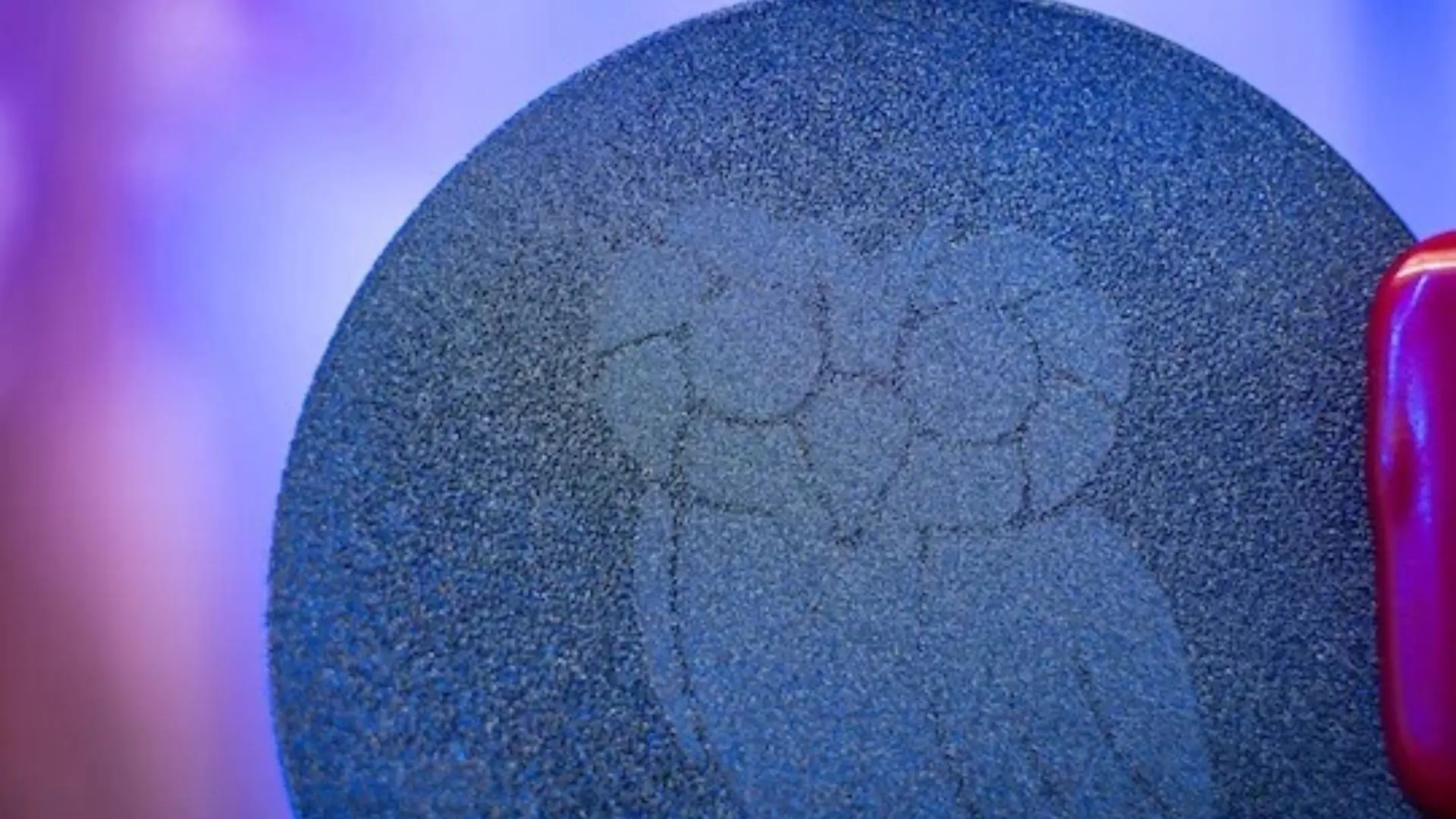
Problems occur when ceramic powders are added to the mix. Ceramics like alumina, zirconia, and silicon carbide remain as small particles in the resin instead of dissolving. These particles and the surrounding liquid bend light differently, leading to a refractive-index mismatch. When UV light hits the material, it scatters in unpredictable directions due to the ceramic particles. The Mie scattering causes stray light to harden the resin outside the intended printing areas. As a result, edges become blurry, features blend, and parts fail to meet size requirements.
When printing features smaller than 100 micrometers, about the width of a human hair, it’s very important to avoid any unintended curing because it can ruin the part. These tiny structures are crucial for modern electronics. Sensors, substrates for 5G antennas, and electromechanical devices all rely on ceramic components made at this scale.
The industrial dyes currently used to address this problem, such as UV327 and Sudan I, are the most common and act via a single mechanism. They absorb excess light but do nothing about the free radicals generated by scattered UV in the resin. Those radicals trigger their own curing reactions independently, producing defects even after the light has been brought under control.
How curcumin solves the problem
Curcumin helps in two main ways. First, it absorbs extra ultraviolet (UV) radiation before it can damage the resin. Second, it acts like a sponge, soaking up harmful molecules created by scattered UV light. It prevents unwanted reactions from starting.
Adding just 0.02 percent curcumin by weight to the resin reduces the intensity of UV-induced free radicals by about 43.6 percent. In alumina slurries, this addition cuts the smallest printable feature size from 66.8 micrometers to 26.1 micrometers. As a result, complex gyroid structures with walls as thin as 50 micrometers can be printed cleanly, without the defects found in control batches.
Twenty-six micrometers is about one-third the width of a human hair. At this small scale, ceramic parts can have internal channels, lattice structures, and features that are hard to create from solid blocks or with standard DLP methods. It can also work with very low amounts, just 0.01 percent by weight, keeping the extra cost low.
Curcumin did not affect the sintering process, during which ceramic particles are heated to form strong finished parts. The final products passed mechanical tests. If an additive improved print resolution but weakened the finished part’s strength, it would not be useful in industry. This one does not.
The applications and why precision matters for each
The main use of silicon carbide is in semiconductor manufacturing equipment. It is used in edge and focus rings in plasma etching chambers to control the electric field during chip etching. These rings are located in vacuum chambers where plasma operates at very high temperatures. Their shape is crucial because it determines where material is removed from a wafer.
At advanced process nodes, such as 3nm and below, even a small flaw in a silicon carbide ring can degrade wafer-level chip yield. Currently, manufacturers produce these components by machining them from sintered ceramic blocks, a slow and expensive process. This process also limits the shapes’ complexity. DLP printing can produce near-net-shape silicon carbide components directly, but it must ensure that scattering does not compromise dimensional accuracy. The curcumin approach specifically aims to improve this aspect.
China plans to become a global leader in electronic ceramics by 2035, including manufacturing materials and components such as multilayer ceramic capacitors, ceramic filters, and low-temperature co-fired ceramic substrates. These are important for 5G base stations and high-frequency defense electronics. The advanced ceramics market grew from about $75 billion in 2018 to over $100 billion in 2023. China now leads in raw material production and mass manufacturing.
Higher-resolution DLP printing helps create more detailed ceramic electronic parts. With this technology, manufacturers can produce smaller capacitors, denser filter arrays, and more accurate antenna substrates, which meet China’s needs in electronics production. In addition, in the aerospace and defense industry, alumina is an important material for missile radomes, which shield radar antennas.
Alumina remains stable at high temperatures and allows radar waves to pass through. High-purity alumina can withstand temperatures above 1,760 degrees Celsius while remaining transparent to radar signals. The shape of the radome matters a lot. Even small changes can affect how air moves around it, change the missile’s path, and lower its accuracy. DLP printing can produce complex radome shapes that are hard to achieve with older methods, but it requires higher resolution than traditional technologies can provide.
Hypersonic vehicles can reach temperatures exceeding 2,200 Kelvin (1,925 degrees Celsius) at their nose tips and leading edges when traveling faster than Mach 5. To protect against this extreme heat, we use silicon carbide ceramic structures. Their design, which includes internal shapes, lattice cores, varying densities, and built-in cooling channels, affects how well they manage heat. Using high-resolution printing allows us to create more precise thermal management designs and reduces material waste. It is important because the components are costly to produce and must be replaced quickly as production increases.
The Chinese context
Research from Hunan University was published in the International Journal of Extreme Manufacturing, which China’s advanced manufacturing research institution supports. China is a leader in the production of advanced ceramics. The country has the necessary raw materials and manufacturing infrastructure for mass production, especially in electronics, aerospace, and defense sectors.
Chinese companies that make advanced ceramics for high-end applications, such as semiconductor equipment, electric vehicle power systems, and high-temperature industrial applications, have a unique opportunity to create significant value as the market grows over the next decade. When a manufacturing improvement comes from a university lab in China, it can be adopted in industry more quickly than in countries without a similar background. The key question is whether this research can move from academic tests to actual production at companies that supply China’s semiconductor equipment and defense electronics. This shift will determine the research’s impact on the industry.
However, curcumin also has limitations that need to be clear. It is used during printing but can deplete quickly under intense light. This rapid depletion can lead to unintended curing of materials. To address this, researchers had to increase the curcumin concentration from 0.01 to 0.015 percent by weight in alumina when using higher-energy UV light. Silicon carbide, which requires stronger light for proper printing, created an even greater challenge by exacerbating scattering issues, even as curcumin helped reduce them.
Curcumin repels water, limiting its use in water-based resin systems without altering its chemical properties. This limitation affects some industrial ceramic printing processes. There is also a challenge with scale. High-resolution DLP systems are designed to work in small build areas. Printing at 26-micrometer precision on larger components, such as a full-size semiconductor equipment ring rather than a lab sample, is a different engineering challenge that this research does not tackle. The first step is to solve the scattering problem at a small scale. The second step is to maintain that solution at a production-scale build volume.
What’s next
The paper demonstrates that the method applies to four types of ceramic materials and provides concentration guidelines for each. However, it does not explain how to use this method in production. It does not detail how to consistently manage curcumin dosing in a commercial DLP ceramic printer throughout a full production run, how to standardize formulations for specific industrial uses, or how to address water compatibility for broader applications.
These are engineering challenges, not scientific ones. The basic chemistry is already known. Getting lab results to the production line involves process engineering, and that work has not yet been publicly announced.
The research addresses a manufacturing problem that reduces the precision of ceramic components in multiple industries. The solution is effective and affordable, and it has been proven to work across different types of materials. It opens up new possibilities for what can be built in semiconductor factories in South Korea and Taiwan, in electronics manufacturing lines in China, and in aerospace production facilities in the region.