Key ideas
- •Japanese physicist Tsumoru Shintake has designed a four-mirror EUV system that could achieve 0.55 numerical aperture with simpler, more manufacturable optics.
- •The design could offer a cheaper alternative to ASML's $360 million to $400 million High-NA EUV machines by using rotationally symmetric mirrors that can be produced with conventional optical manufacturing techniques.
- •The concept remains unproven in hardware, with 35 to 37 percent central obscuration and lower throughput from its stepper design creating major engineering challenges before it can compete with ASML.
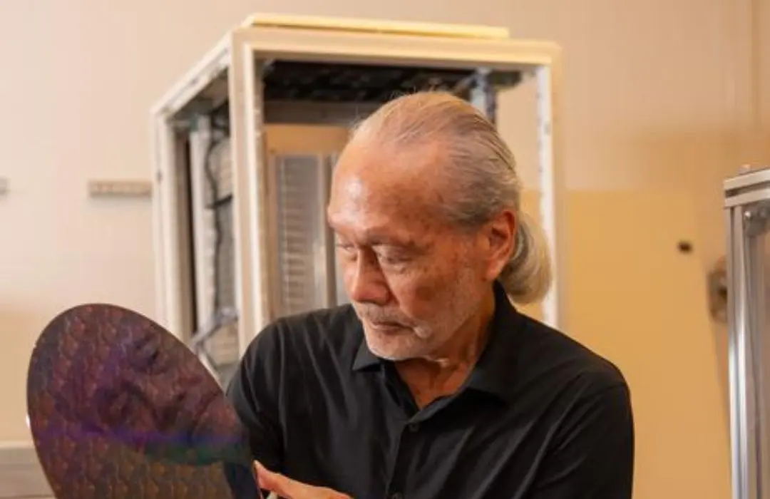
Every computer chip starts as a beam of light. In the machines that make the world’s advanced semiconductors, this light needs to be focused very precisely, creating features just a few nanometers wide, much smaller than a human hair. For years, engineers have had to deal with an optical flaw that drives up costs and limits precision. Now, a physicist in Okinawa, Tsumoru Shintake, claims to have found a simpler solution that could change how the industry builds its most expensive machines.
Shintake works at the Okinawa Institute of Science and Technology. His design, recently published in the Journal of Micro/Nanopatterning, Materials and Metrology, uses four mirrors arranged in two stages to focus extreme ultraviolet (EUV) light, which is essential for modern chipmaking. His design causes much less distortion than current systems.
Understanding the importance of this improvement requires knowing the costs of existing systems. ASML, a Dutch company, has a near-monopoly on EUV lithography machines. The company sells its standard EUV systems for $150 million to $200 million each. Its latest High-NA EUV machines, which aim for the same precision that Shintake’s design achieves, cost about $360 million to $400 million each. Each machine arrives in 40 containers and needs to be assembled on-site by ASML engineers.
The mirrors used in these machines are made exclusively by Carl Zeiss SMT in Germany, under a strict agreement with ASML. The arrangement prevents any competitor from making EUV machines without access to Zeiss’s optics. On the other hand, Shintake’s design uses symmetric mirrors around a central axis, similar to a telescope lens. This is simpler than the complex shapes that Zeiss produces for ASML.
Symmetric mirrors can be made and checked using standard optical manufacturing methods. This is especially important for Japanese and South Korean companies that want to build EUV equipment without relying on ASML and Zeiss.
The problem
The main issue with today’s EUV systems is called the mask 3D effect. In these machines, light hits the photomask, or stencil for the chip, at an angle. The angle causes the light to cast small shadows and misalign features because the mask is physically thick. These errors grow as engineers try to fit more details onto the chip.
Shintake’s design solves this problem by sending light directly at the mask instead of at an angle, removing the distortion right at the source rather than trying to fix it later.
Additionally, the design includes a self-correction feature. It works in two steps, where errors made in the first step are corrected in the second. This redundancy helps the system keep its performance high, even at fine resolutions, without needing the extremely precise manufacturing that makes ASML’s mirrors so costly to produce.
The physics
The main engineering problem with Shintake’s design is that each mirror in its four-mirror setup has a hole in the centre. These holes block some of the light before it reaches the wafer. In Shintake’s two top designs, this blockage, known as central obscuration, is up to 35 per cent for the lower-resolution version and 37 per cent for the higher-resolution version.
On the other hand, ASML’s ring-field design allows light to go around the edges of each optical element, letting it reach the wafer with almost no central obscuration. The difference is important because it is already hard and expensive to generate EUV light. ASML’s machines create EUV by firing a laser at tiny drops of molten tin, vaporising them at a rate of 50,000 times per second.
Each usable photon of light from this process requires a lot of engineering effort. If Shintake’s design wastes 35 to 37 per cent of the light before it reaches the chip, it either reduces the machine’s productivity compared to ASML’s systems or needs a more powerful light source to make up for it.
Shintake’s light source is being developed alongside the design. Researchers at Kyung Hee University’s C-Beam Laboratory in South Korea shared early findings in April at the Photomask Japan meeting. Their method shoots an electron beam from a carbon-nanotube cold cathode at a solid tin target to produce EUV light suitable for chipmaking.
The source, powered by a 20-kilowatt beam, is expected to generate about 300 watts of usable EUV power. To stop the tin target from melting during continuous use, engineers rotate it on a spinning anode, which lowers peak temperatures at the impact point. Whether 300 watts can compensate for the central obscuration loss and keep productivity competitive in a production setting is one of the questions that a physical prototype needs to answer.
The stepper trade-off
ASML machines, used today, are designed as scanners. They continuously move the wafer under a light beam, allowing for fast processing of large areas.
In contrast, Shintake’s design uses a stepper, which exposes one section of the chip at a time. The semiconductor industry switched from steppers to scanners because scanners produce more wafers every hour, and this production speed is crucial for the economics of a chip factory.
Shintake believes this speed difference is less important now. Many chipmakers are using smaller chiplets to build processors instead of creating one large piece. The approach reduces the need for wide exposure fields.
He also suggests that chipmakers could use several of his simpler machines working at the same time to match the output of one ASML scanner. While this idea is reasonable given the cost difference, it also requires more space, more maintenance, and more coordination than his paper discusses.
The competitive landscape
Shintake is not the only person working on an alternative to ASML. xLight, a startup in the US led by Pat Gelsinger, the former Intel CEO, is creating EUV sources using free-electron lasers. These sources could reach wavelengths as short as two nanometres, which is much finer than what current machines can do.
In December 2025, Reuters reported that China had finished a prototype EUV machine in Shenzhen, made by SMEE with government funding. They expect to produce working chips between 2028 and 2030. Huawei has also filed patents related to EUV technology.
Shintake’s design aims to replicate ASML’s resolution but does not try to exceed ASML’s wavelength. His goal is to offer a lower-cost solution using simpler optics that manufacturers outside the ASML-Zeiss partnership can build.
The Japan angle
Shintake’s design aims to give Japanese and Asia-Pacific chipmakers a competitive edge. Japan’s electronics and materials industry can provide many of the components needed for this system. One key component is cordierite ceramic, which is known for its minimal thermal expansion and is produced by Kyocera, a Japanese electronics company. Another important material is silicon carbide, which is already made by Japanese manufacturers and is used in mirrors for space telescopes.
The unique shape of Shintake’s mirrors allows them to be made and tested using standard optical polishing and inspection equipment. This is different from the special techniques developed by Zeiss for ASML’s mirrors. A Japanese optics manufacturer that can produce telescope mirrors with space-grade accuracy already has the tools necessary to create Shintake’s mirrors, but they cannot make ASML’s mirrors.
Shintake’s design builds on his previous research with physicist Patrick Naulleau about cost-effective, energy-efficient EUV lithography. It also relies on Shintake’s experience in high-energy physics, which includes helping with the SACLA X-ray free-electron laser and a microwave undulator at KEK, Japan’s high-energy accelerator research organisation.
His knowledge about cooling systems for particle accelerators helped shape the water-cooling design in the mirror assembly, which keeps mirror temperatures steady within one thousandth of a degree.
The leftover
The design is currently just on paper. Shintake used OpTaliX optical design software to create a model of the mirror system under perfect conditions, ignoring real-world issues like polarisation effects and problems caused by coatings. No physical hardware has been made yet.
Simulations of the four-mirror setup showed it achieving a numerical aperture of 0.55, with optical errors much smaller than a thirtieth of a wavelength. It has a patterning field of 21 by 21 millimetres. The design allows for telecentric illumination, meaning light hits the chip at a consistent straight angle. It reduces the 3D effect of masks geometrically instead of through software corrections. By tilting one mirror, engineers can switch between different lighting patterns for various circuit features, which adds flexibility without needing more hardware.
Shintake’s next step is to build a physical prototype. A patent application titled “Optical system and projection exposure device” has been submitted in Japan. The change from simulation to real hardware often stops many promising optical designs. Mirrors that look good in models can develop issues like thermal stress, surface changes, and uneven coatings that were not considered in the simulations.
The M2 mirror, which is closest to the wafer and causes the most central obscuration, is the hardest part. Moving it closer seems like an easy fix, but it requires making it thinner. However, thin mirrors can warp under heat when precision is needed.
Whether this design will benefit the chip industry depends less on the physics, which seem solid in the simulation, and more on a fabrication team in Japan, South Korea, or another location deciding to build the prototype. The cost of $360 million per ASML High-NA unit makes a cheaper alternative very appealing. However, the engineering challenges are significant.